QUALITY CONTROL STEPS DURING PROCESS
Defective PCBs are discarded or repaired (except IPC-A-600 class 3) for compliance.
Here is the table summarizing the quality checks carried out during the process.
| Control | Equipment | PCB type / option | class 2 | class 3 | |
|---|---|---|---|---|---|
| 1.0 - Customer technical files (gerber) | Digital image | Safe gerber viewer | All PCBs | Yes | Yes |
| 2.0 - Safe-PCB manufacturing files | Netlist compare | CAM350 function | All PCBs | Yes | Yes |
| 3.0 - Laminate cut | Copper/insulator thickness control | Copper thickness meter / magnetic induction | All PCBs | Yes | Yes |
| 4.0 - Drilling | Tool diameter control | Laser measurment on machine | All PCBs | Yes | Yes |
| 4.1 - Drilling | Hole diameter after drilling | Tunnel hole checker | All PCBs | Yes | Yes |
| 5.0 - Etching | Internal layers etching quality | AOI | All multilayers | Repair accepted | No repair accepted |
| 5.1 - Etching | External layers etching quality | AOI | All PCB | Repair accepted | No repair accepted |
| 6.0 - Press | Dimensional measurement | ASIDA - optical control | Multilayers / blind holes | Yes | Yes |
| 6.1 - Press | Layers alignement | ASIDA -X-RAY control | Multilayers / blind holes | Yes | Yes |
| 7.0 - Metallization | Copper thickness measurement | Thickness measurement probe | All PCBs | Yes | Yes |
| 8.0 - Soldermask | Soldermask quality | Visual inspection | All PCBs | Yes | Yes |
| 9.0 - Electrical test | Open/short circuits | Flying probe test or pin mould | All PCBs | Yes | Yes |
| 9.1 - Electrical test | Resistance control | Resistive probe test | Multilayers / blind holes | Yes | Yes |
| 10.0 - V-CUT | Depth V-CUT control | Depth gauge | All PCBs | Yes | Yes |
| 11.0 - Milling | Dimension control | Calipers | All PCBs | +/- 150 µm | +/- 150 µm |

PCB checked using this procedure : 100% of PCB.
Safe-PCB asks the customer to validate their PCB design after it's checked by our technicians.
Safe-PCB provides a digital image of the final PCB result to the customer at this step of the process.
An order can NOT be produced without previous customer GERBER validation.
PCB checked using this procedure : 100% of PCB.
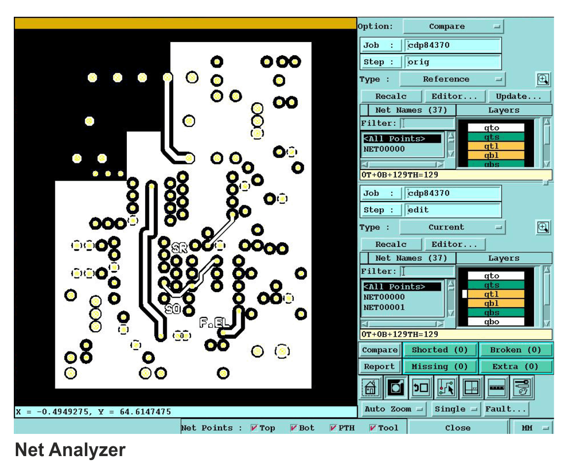
Before production of the PCB in our factory, every order's manufacturing file is checked by our technicians to make sure it's totally conform to the original GERBER file provided.
This is done by a software function called Netlist compare, which compares the original GERBER file and manufacturing file.
PCB checked using this procedure : 100% of PCB.
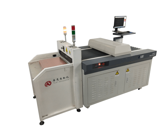
After drilling, Safe-PCB optically checks the holes diameter.
This test is done using a semi-automatic equipment (Picture on the right) that compares it to the drillmap provided with the GERBER file.
Each drilled hole is controled with this equipment.
PCB checked using this procedure : all multilayer PCB.
The AOI test is used to check multi-layer boards.

PCB checked using this procedure : 100% of multilayer PCB containing blind holes.
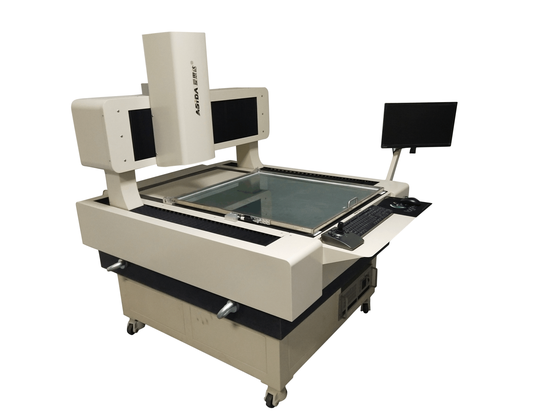
PCB with blind holes need a perfect layer alignment. Safe-PCB checks these PCB using two complementary equipments:
. One optical ASIDA equipment that controls the PCB before the pressing step
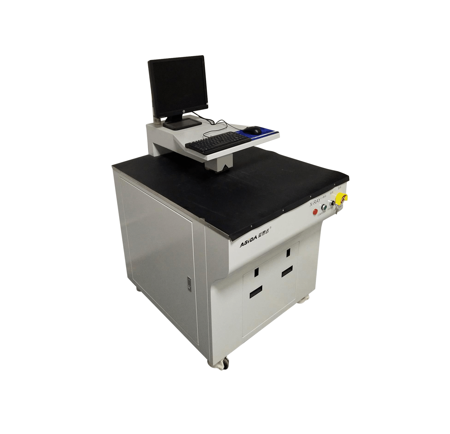
. One X-Ray ASIDA equipment that controls the PCB after the pressing step
The optical equipment (Picture on the right) allows Safe-PCB to control the internal layers dimensions before pressing, preventing bad alignment of holes and copper tracks
In addition to the ASIDA machine, Safe-PCB checks these PCB using a X-ray machine.
This equipment irradiates the PCB with X-rays allowing Safe-PCB technicians to control the alignment of inner layers after the pressing step with a camera. This system is similar to a medical X-Ray radiography.
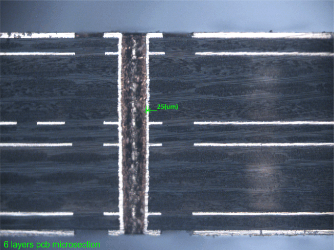
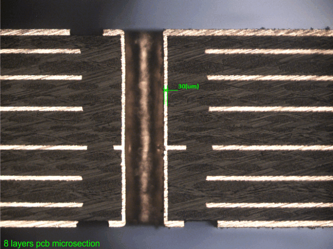
PCB this procedure applies to : 100% of multilayer PCB.
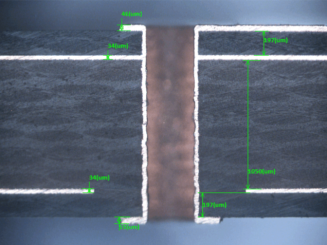
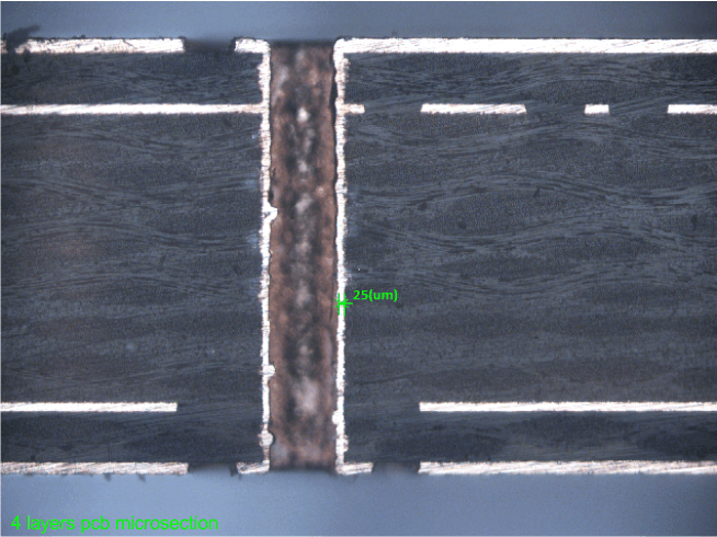
This step of the process takes place after applying the surface finish on the PCB. A technician cuts a small piece of panel and checks :
. Copper layers thickness
. Hole copper thickness (PTH)
. PP (Prepreg) layers thickness
He then reports these measures on the picture of the microsection.
During the final quality control step the picture of the microsection is uploaded to the quality control report.
Microsections of 4...8 layers PCB below.

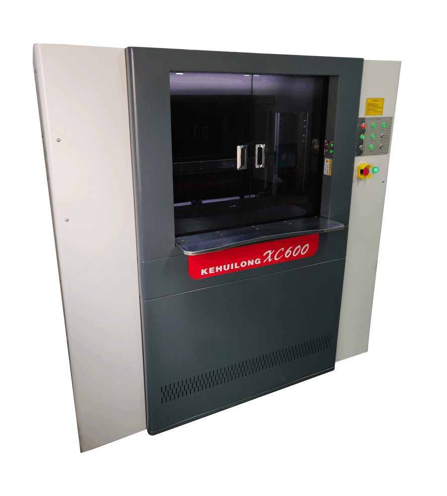
Prototypes and small series undergo E-test performed using flying probe testers. Safe-PCB currently uses 9 flying probe testers :
- 5 ADLONG KS1000 testers
- 3 KEHUILONG XC 600 testers
- 1 SPACELIGHT ESL618-L tester
Larger series are tested using a testing framework needle - requires the manufacture of a dedicated file for each manufacturing equipment. Safe-PCB currently uses 2 of these :
- 1 KEHUILONG KHL910 tester
- 1 WTD HV300
Recommend
-
-

QQ Zone
-

Sina Weibo
-

Renren.com
-

Douban