COPPER THICKNESS - COPPER PROCESS
Single layer PCBs
. No metallization process
. Tracks and copperplates are obtained by a simple etching operation.
. Copper thickness depends on the choice of copper foil from the laminate supplier. Standard thicknesses: 17.5 / 35/70/105/140/210 µm ...
Double side PCBs - 2 layers with metallized holes (PTH)
. Hole metallization process
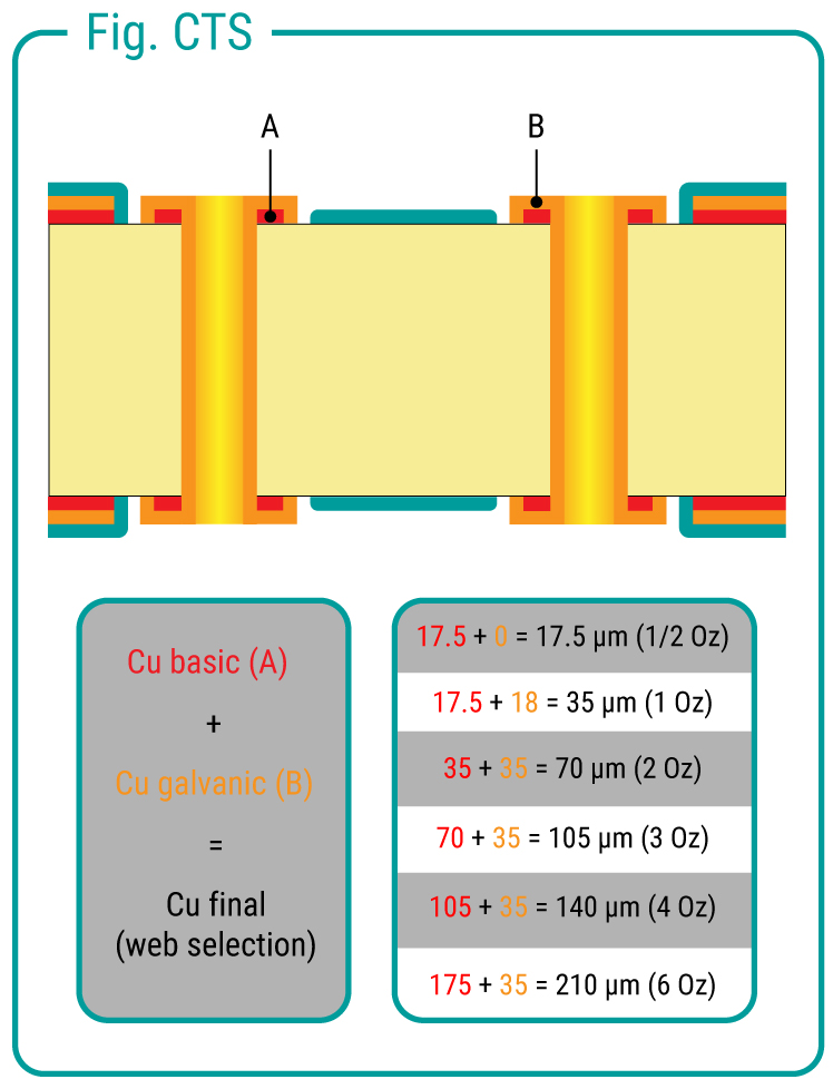
. Final thickness results from the addition of 2 copper layers: Base copper + Copper refill on the tracks and ground planes during the hole metallization process (PTH).
. Example: 17.5µm (1 Oz - Cu base) +. 17.5 µm (1 Oz - Cu refill) = 35 µm finished copper.
For "RIGID - 2 layers PCBs", 35µm copper finished on the outer layers is the standard thickness, therefore the most economical.
Multilayer PCBs (standard)
. Internal layers: No metallization process - Copper tracks and planes are obtained by a simple engraving operation.
. External layers: Final thickness results from the addition of 2 layers of copper: Base copper + Copper refill
Multilayer PCBs with buried and/or crossblind holes
. Internal layers: Without metallization process - Copper tracks and planes are obtained by a simple etching operation.
. Internal layers: With metallization process - Addition of 2 copper layers: Base copper + Copper refill.
. External layers: Final thickness results from the addition of 2 layers of copper: Base copper + Copper refill
All these configurations are detailed in the menus below.
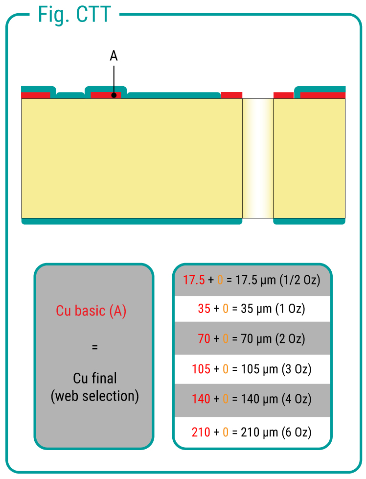
For single-sided PCB, base copper thickness and finished copper are the same. Indeed, not having holes to be metallized (no PTH), there is no metallization step.
The tracks are obtained only by chemical etching of the copper layer.
Base Cu thickness = finished Cu thickness.
The table (fig. CTT) shows the list of thicknesses available on the website.
This 25 µm copper recharge lead to a slightly higher finished copper thickness on tracks and copper planes:
For a selection Cu = 35 µm on the web configurator, the final thickness generally measured is Cu = 42.5 µm resulting of 17.5 (Cu base A) + 25 (Cu recharge B)
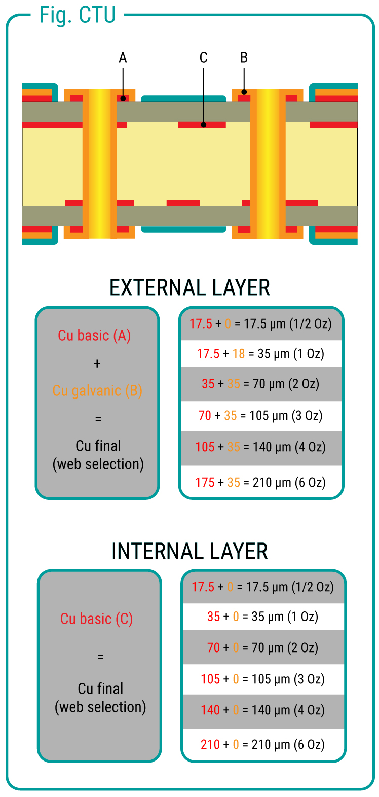
For standard multilayers (1 press cycle), the external and internal finished copper thicknesses are not calculated in the same way.
For the outer layers, like the double side PCBs, it is necessary to take into account:
Base thickness (A) + Metallization thickness (B).
For the internal layers, like the single side PCBs, there is no metallization:
Base thickness (C) = Finished thickness
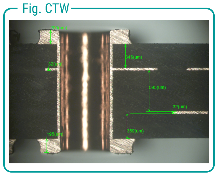
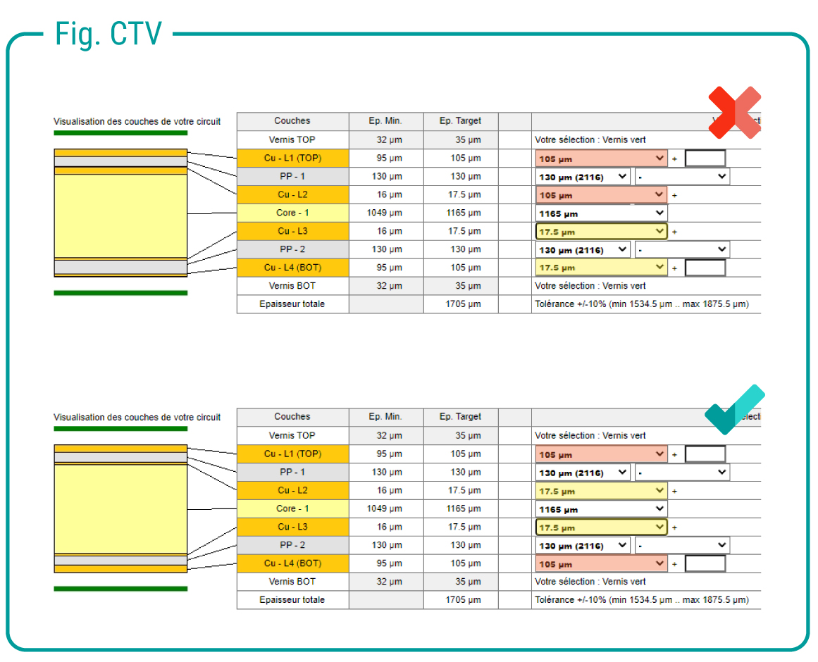
The external and internal thicknesses can be different, but it is necessary to respect a symmetry of the thicknesses on the Stackup (Fig CTV and CTW).
See the Stackup section for more information on this, our online tool allowing you to configure feasible stackups.our
For complex multilayers (several pressing cycles), the position of the buried, blind or crossed holes will determine on which layer (s) of the stackup a copper refill is necessary.
Examples of complex stackup are in preparation. Online soon.

Recommend
-

-

QQ Zone
-

Sina Weibo
-

Renren.com
-

Douban