PEELABLE MASK
PEELABLE MASK
The peelable mask will hide a defined portion of the PCB and can be removed easily.
It must be able to withstand 2 or 3 welding processes without detaching it from the PCB.
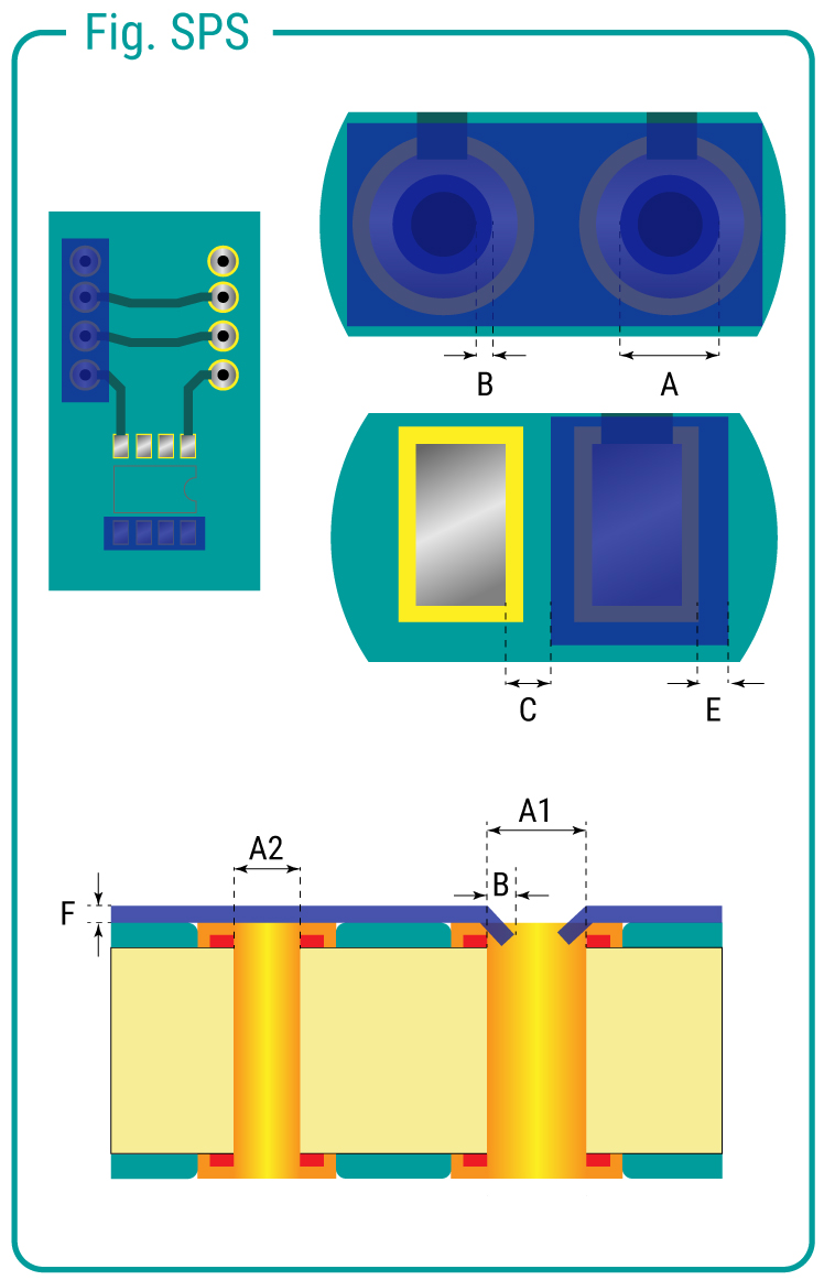
The peelable mask is shown in blue. (Fig SPS).
. Minimum overlap both sides of an element to hide (pad, via, etc. ..): 0.6 mm (E - Fig.SPS)
. Minimum space between the edge of the peelable mask and anything not covered: 0.6 mm (C - Fig.SPS) .
. Minimum width : 2 mm.
. Holes Ø < 3 mm (A2 - Fig.SPS) completely hidden..
. Holes Ø > 3 mm (A1 - Fig.SPS) partially hidden..
. Overhang soldermask inside the hole: 0.6 mm (0.3 + 0.3 = 0.6). (B - Fig.SPS).
. Peelable mask thickness > 0.25 mm . (F - Fig.SPS).
Where to find this option (quote and or order page):
Recommend
-

-

QQ Zone
-

Sina Weibo
-

Renren.com
-

Douban